Accumulator Shifting Unit 2
Accumulator
Main Adder
Computer Control I
Computer Control X
Computer Control II
Computer Control III
Computer Control IV
Computer Control V
Computer Control VI
Computer Control VII
Computer Control VIII
Computer Control IX
Coincidence Unit
Clock Generator
Complementer/Collater
Control Switches and Logic
Counter
Digit Pulse Generators
Engineers Control Panel
Frigs
Half Adder Type 1
Half Adder Type 2
Main Control Unit
Multiplicand Tank
Memory Units
Multiplier Tank
Order Coder
Order Decoder 1
Order Decoder 2
Order Flashing Unit
Order Tank
Printer
Sequence Control Tank
Initial Orders Loader
Timing Control Tank
Tank Address Decoder 0
Tank Address Decoder 1
Tank Address Distribution
Tank Address Flashing Units
Tank Address Decoding Final Stage
Tape Reader
Test Frigs
Transfer Unit
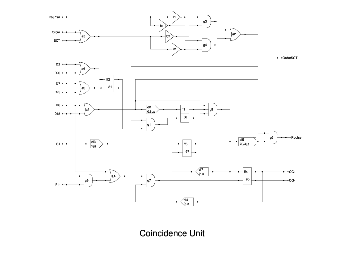
The Coincidence Unit (CU) is crucial to all references to the memory tanks. Since the tanks are mercury delay lines, the only way to determine the position of a word within the line, is to use a Counter Tank which simply counts up by one for each half cycle. When the counter matches the desired address the Coincidence Unit detects this and treats the following half cycle or full cycle as the desired data.
This process is used in both stages of an instruction; in the first part where the instruction itself is being sought, and in the second part where some data is required to be transferred either from or to the store.
The two main inputs to the CU are SCT and Order. These are gated in their respective modules, so that SCT only appears during stage 1 (instruction fetch), while Order is present only during stage 2 (execution). As a result, these are simply OR'd together and during the period of D2 to D6 they are compared with Counter. The gates g1 to g4 and a2 form a simple comparator, with any differences being used to reset ff1.
The flipflop ff1 is set by digit pulses D0 and D18 and the positive output is gated with D17 and D35. In the event of a match, then this pulse triggers the coincidence gate flipflop ff4 which opens the appropriate memory gate to allow a transfer to or from the memory.
The coincidence gate is reset, either by D35, or if the instruction length bit is zero, as indicated by F1-, then by D17.
The whole process of detecting a coincidence is triggered by the stimulating pulse S1 which is generated by the MCU.
The logic for this unit is basically that of Figure 6 of the Report, but with some significant timing changes. In order to get the Coincidence Gate signal (CG+) opening soon enough to access the correct data from the memory tanks, I had to move a number of events forward in time, and used D35 and D17 in place of D0 and D18 in places. A number of additional timing adjustments then had to be made to get things back into the correct timing. Hopefully, these can be eliminated in the replica.
Figure 6 shows a negative Coincidence Gate signal being produced but I have found no use for this, so it can be omitted if desired.